- 您现在的位置:买卖IC网 > Sheet目录333 > IRS2117PBF (International Rectifier)IC DRIVER MOSFET/IGBT 1CH 8-DIP
IRS211(7,71,8)(S)
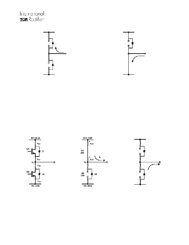
DC+ BUS
DC+ BUS
Q1
OFF
D1
Q1
OFF
D1
I L
V S
V S
I L
Q2
OFF
D2
Q2
ON
DC- BUS
Figure 8: D1 conducting
DC- BUS
Figure 9: Q2 conducting
However, in a real inverter circuit, the V S voltage swing does not stop at the level of the negative DC bus,
rather it swings below the level of the negative DC bus. This undershoot voltage is called “negative V S
transient”.
The circuit shown in Figure 10 depicts a half bridge circuit with parasitic elements shown; Figures 11 and 12
show a simplified illustration of the commutation of the current between Q1 and D2. The parasitic inductances
in the power circuit from the die bonding to the PCB tracks are lumped together in L D and L S for each switch.
When the high-side switch is on, V S is below the DC+ voltage by the voltage drops associated with the power
switch and the parasitic elements of the circuit. When the high-side power switch turns off, the load current can
momentarily flow in the low-side freewheeling diode due to the inductive load connected to V S (the load is not
shown in these figures). This current flows from the DC- bus (which is connected to the COM pin of the HVIC)
to the load and a negative voltage between V S and the DC- Bus is induced (i.e., the COM pin of the HVIC is at
a higher potential than the V S pin).
DC+ BUS
Q1
OFF
V S
+
D1
Q2
OFF
_
+
_
V LD2
V LS2
D2
I L
DC- BUS
Figure 10: Parasitic Elements
Figure 11: V S positive
Figure 12: V S negative
In a typical power circuit, dV/dt is typically designed to be in the range of 1-5 V/ns. The negative V S transient
voltage can exceed this range during some events such as short circuit and over-current shutdown, when di/dt
is greater than in normal operation.
International Rectifier’s HVICs have been designed for the robustness required in many of today’s demanding
applications. An indication of the IRS211(7,71,8)’s robustness can be seen in Figure 13, where there is
represented the IRS211(7,71,8) Safe Operating Area at V BS =15V based on repetitive negative V S spikes. A
negative V S transient voltage falling in the grey area (outside SOA) may lead to IC permanent damage;
viceversa unwanted functional anomalies or permanent damage to the IC do not appear if negative Vs
transients fall inside SOA.
www.irf.com
12
? 2008 International Rectifier
发布紧急采购,3分钟左右您将得到回复。
相关PDF资料
IRS2124STRPBF
IC DVR HI SIDE 600V 500MA 8-SOIC
IRS21271STRPBF
IC DVR CURRENT SENSE 1CH 8-SOIC
IRS21531DSTRPBF
IC DRVR SELF-OSC HALF BRG 8-SOIC
IRS21814MPBF
IC DRIVER HIGH/LOW SIDE 16MLPQ
IRS2181STRPBF
IC DRIVER HI/LO SIDE 600V 8-SOIC
IRS21834STRPBF
IC DRIVER HALF-BRIDGE 14-SOIC
IRS21844MPBF
IC DRIVER HALF-BRIDGE 16MLPQ
IRS2184PBF
IC DVR HALF BRIDGE 8-DIP
相关代理商/技术参数
IRS2117PBF
制造商:International Rectifier 功能描述:MOSFET Driver IC
IRS2117SPbF
功能描述:功率驱动器IC 1 NONINVERTING INPUT VTG THRESHOLD RoHS:否 制造商:Micrel 产品:MOSFET Gate Drivers 类型:Low Cost High or Low Side MOSFET Driver 上升时间: 下降时间: 电源电压-最大:30 V 电源电压-最小:2.75 V 电源电流: 最大功率耗散: 最大工作温度:+ 85 C 安装风格:SMD/SMT 封装 / 箱体:SOIC-8 封装:Tube
IRS2117SPBF
制造商:International Rectifier 功能描述:MOSFET Driver IC
IRS2117STRPBF
功能描述:功率驱动器IC Sngl Hi Sd Drvr NonInvrt Inpt RoHS:否 制造商:Micrel 产品:MOSFET Gate Drivers 类型:Low Cost High or Low Side MOSFET Driver 上升时间: 下降时间: 电源电压-最大:30 V 电源电压-最小:2.75 V 电源电流: 最大功率耗散: 最大工作温度:+ 85 C 安装风格:SMD/SMT 封装 / 箱体:SOIC-8 封装:Tube
IRS2118
制造商:IRF 制造商全称:International Rectifier 功能描述:SINGLE CHANNEL DRIVER
IRS2118PBF
功能描述:功率驱动器IC Sngl Hi Sd Drvr Invrt Inpt RoHS:否 制造商:Micrel 产品:MOSFET Gate Drivers 类型:Low Cost High or Low Side MOSFET Driver 上升时间: 下降时间: 电源电压-最大:30 V 电源电压-最小:2.75 V 电源电流: 最大功率耗散: 最大工作温度:+ 85 C 安装风格:SMD/SMT 封装 / 箱体:SOIC-8 封装:Tube
IRS2118PBF
制造商:International Rectifier 功能描述:MOSFET Driver IC
IRS2118SPbF
功能描述:功率驱动器IC 1 NONINVERTING INPUT VTG THRESHOLD RoHS:否 制造商:Micrel 产品:MOSFET Gate Drivers 类型:Low Cost High or Low Side MOSFET Driver 上升时间: 下降时间: 电源电压-最大:30 V 电源电压-最小:2.75 V 电源电流: 最大功率耗散: 最大工作温度:+ 85 C 安装风格:SMD/SMT 封装 / 箱体:SOIC-8 封装:Tube